PCB: choose the type of VIA FILLING according to your needs
When we talk about Via Filling in PCBs, we mean a filling process of vias holes using materials usually dielectric/isolating (but not only) for the purpose of:
• Protect hole metallization
• Prevent the passage of liquid or gas through holes themselves
• Impede the way up of tin during wave soldering
• In case of conformal coating on one side of the board to avoid flows of resin on the opposite side
Such sealing can be obtained using different procedures, in consequence of those results will be different too. Alba PCB Group proposes two possibilities:
• PSR Via Fill: Vias sealing through extra solder resist application (with photographic definition) using a dedicated drawing of solder mask.
• RESIN Via Fill: sealing obtained through specific epoxy resin application (with no photographic definition) considering whether or not an over-coverage of a metallic or of solder resist or of both of them is need.
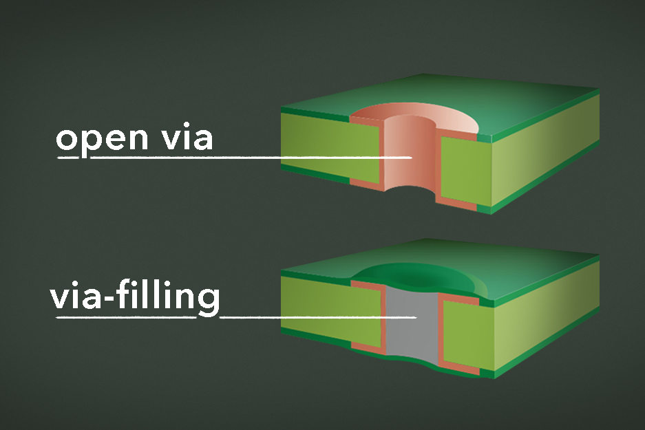
Filling with solder resist (for drilled diameter lower or equal to 0,4mm)
The occlusion of the hole has been obtained through an additional printing of solder resist in correspondence of vias, using a specific stencil realized in a drilled aluminum plate. This technique can guarantee a suitable result for drilling of 0,4mm diameter and lower, but it is not suggested for bigger size holes, due to chemical – physical features of the employed material (LPI).
Over 0,4mm diameter, hole sealing is not guaranteed, since it may become receptacle of chemical compounds which can create some problems in phase of soldering and lost of reliability in the long term.
Even in holes with lower diameter, the usual loss of volume of the employed material during its polymerization, leads to the formation of solder resist material gaps/voids/cracks inside holes, which even though sealed, do not present a whole filling.
Filling with resin (for drilled diameter to 0,7mm)
The occlusion of the hole occurs through a specific process of resining with material one- or two- component, but of screen printing type (so without of direct photographic definition): the typology of the material and the adopted application process assures the complete fill of the hole and with it, its sealing.
> Download .pdf file including all technical details on via filling <
Otras publicaciones

Checking quality looking “2000 times” more!
We don’t take our eyes off from quality! Our control department is the place where...
leer más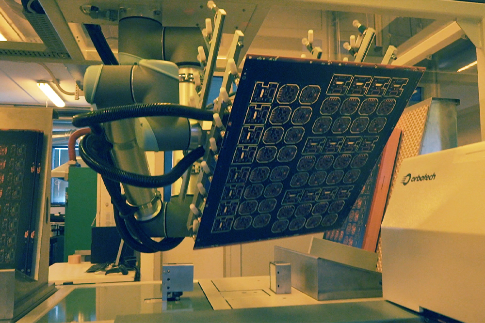
An automated robot for high definition Inkjet silkscreen printing
In our Italian production plant we continue to integrate Hi-Tech solutions that improve production quality...
leer más
Crisis: when PCB supplier becomes strategic…
When PCB supplier becomes strategic to manage PCB supplying risks in a crisis situation. Many...
leer más