The new shadow line for a perfect metallization of micro- and blind holes
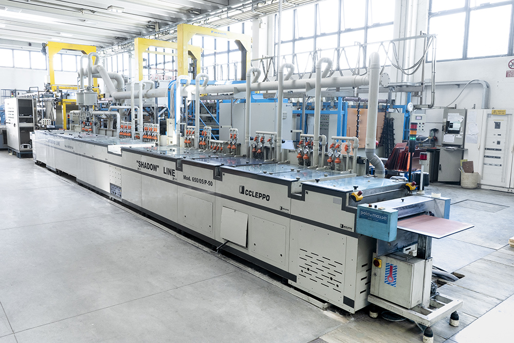
Fifteen meters of automatic horizontal line for removing all the impurities from the holes, making them conductive through the graphite deposit. A process that improves depositing the copper electrolytic in the holes thanks to the 30% increase in the spreading speed of the galvanic copper. A process that ensures a perfect metalizing.
When drilling holes in the dielectric materials, the high temperature reached by the tools generates a residue of dissolved resin on the walls of the holes (smear). The first part of the new line removes this residue. Thus, within the line there is a homogeneous chemical process for the removal of any impurities present on the wall of the holes (de-smearing).
The second part of the line deposits a thin layer of graphite (pre-metalizing shadow) on the walls of the hole just treated, by means of a forced pump process.
The line allows for treating most types of PCBs (rigid, semi-flexible, HDI) made with different types of basic materials (standard FR4, medium and high TG, high CTI, Radio Frequency laminated). It permits a high level of productivity, bringing two exceptional advantages for each type of hole when compared to other metalizing processes:
• Perfectly uniform final metalizing of micro-holes and blind holes, because the process ensures a greater spreading speed for the copper which is subsequently given a galvanic finish.
• Increased reliability of multilayer electrical connections: the reduced graphite deposit requires a smaller micro-incision (less than 4 microns) and therefore a smaller retraction of the intermediate metal layers in the multilayer connections.
Otras publicaciones
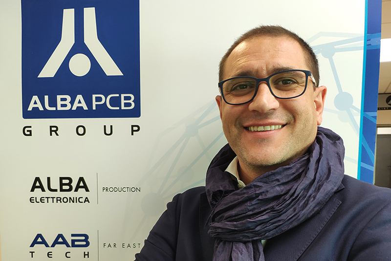
Fabio Puccia Modica is the new Commercial Director
New commercial development strategies for Alba PCB Group. We decided to invest in the development...
leer más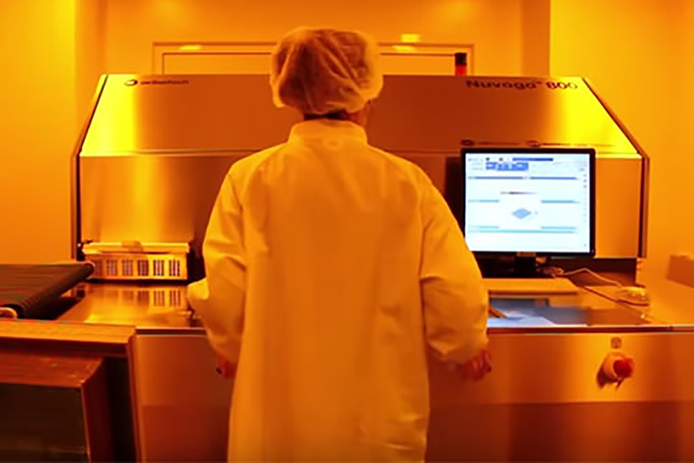
Direct Imaging
We have further enhanced our productive department investing in the most advanced technology for pcb...
leer más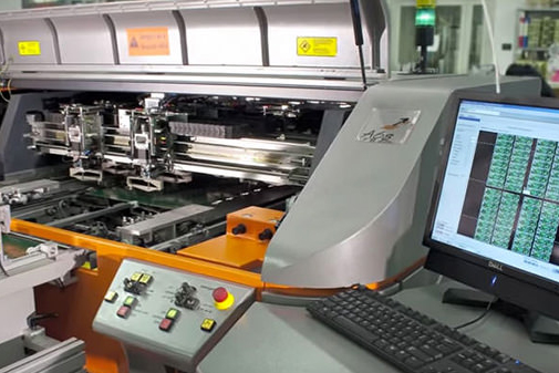
Flying Probe Test ATG A6
Speed, precision and delivery of high quality products! We have invested in an ATG-A6 machine...
leer más