Using blind vias in PCBs avoiding criticalities
Guidelines for using blind vias.
BLIND VIAS AND CONSTRUCTION PARAMETERS
Blind vias are plated-through holes that connect the external layer of a printed circuit board with internal ones without going through the entire PCB.
The hole is drilled on the Z-axis, and its diameter must ensure optimal metal coating on the walls.
5 parameters help you choose a suitable blind via diameter and thus ensure quality and reliability over time.
/5/ PARAMETERS TO CONSIDER WHEN USING BLIND VIAS
To avoid criticalities and ensure durability, the PCB design must consider:
1. Drill size (hole diameter)
2. The size of the copper pad connected to the blind via
3. The thickness of dielectric material between the layers connected through the blind via plus the copper layer
4. The Aspect Ratio of the hole
5. The insulation thickness of the underneath layer not connected to the hole (mechanically-drilled holes only)
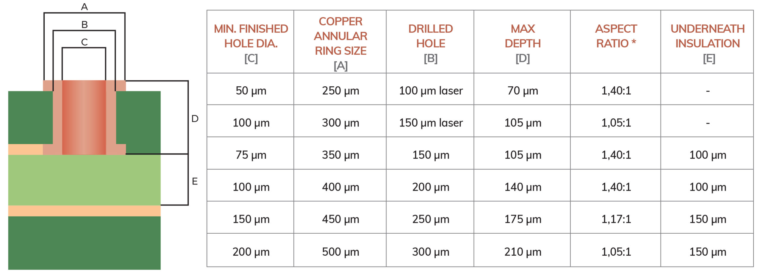
1 – HOLE DIAMETER
Blind via holes can be laser or mechanically drilled:
– A MECHANICALLY-DRILLED HOLE can be made using a tool with a minimum diameter of 0.15 mm (with a negative tolerance of 50 µm). This way, after the metallisation process, you can obtain a hole with a 0.05 mm diameter (or slightly larger).
– A LASER-DRILLED HOLE has a diameter of 0.1 mm (without negative tolerance) to obtain a hole with a 0.05 mm diameter (or slightly smaller).
Please note: a plated blind hole includes the CU plated wall with a minimum thickness of 12 µm, as indicated in the IPC standard.
2- SIZE OF COPPER PAD CONNECTED TO THE BLIND VIA
The blind via pad must have a diameter of at least 300 µm (11.8mls) larger than the blind via diameter (after CU plating – considering layers with a copper thickness of 35 µm) to comply with IPC standards and ensure an optimal PCB.
This aspect is essential for centring the hole on blind via pad while maintaining the required hole size.
For laser-drilled holes, this value can be reduced to 250 µm (10 mls).
3- INSULATION THICKNESS BETWEEN THE 2 LAYERS CONNECTED THROUGH THE BLIND VIA
The thickness of the insulators and conductive layers depend on electrical design requirements. This also applies to the layers involved in blind vias. (It is related to the Aspect Ratio).
4- ASPECT RATIO (AR) – (after CU plating)
Aspect ratio refers to the ratio between the hole’s depth and hole’s diameter.
Note:
– The hole’s depth is given by the dielectric thickness between 2 connected layers plus the copper layer thickness;
– The hole’s diameter is after CU plating.
Aspect Ratio is important due to the chemical, physical and fluid-dynamic limits of the electrolytic plating process applied to the holes. During the galvanic coating process, different liquids must flow inside a cylinder created by the blind drilling.
This process is carried out to obtain a durable metal coating of the hole wall and a reliable electrical connection.
This ratio must be a maximum of 1.4:1.
i.e., the diameter of the annular rings must depend on the thickness of the dielectric and copper layers (hole depth maybe only slightly wider than the hole diameter).
5- INSULATION THICKNESS BENEATH THE HOLE (mechanically-drilled holes only)
It refers to the dielectric thickness between the second layer connected to the blind via and its adjacent inner layer (underneath), which is not connected. According to the tolerances required by the Z-axis-controlled drilling process and the shape of the drilling tool, this thickness must ensure correct electrical insulation at the end of the process.
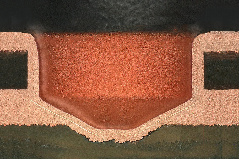
EXAMPLEOF A RELIABLE BLIND VIA
Suppose you have a PCB with 35 µm-thick copper layers, where 100 µm of dielectric material insulate the top and the first inner layer, and 150 µm (E) of material insulate the second inner layer. In this case, you can engineer a blind via with a 150 µm diameter (C) (no laser) centred on copper pad having a diameter of 450 µm (A). This hole is made with a 250 µm-diameter tool (B), which crosses a material thickness (FR4 + copper layer) equal to 170 µm (D). This way, AR reaches 1.13:1 (D/C), which is lower than 1.4:1. This ensures excellent performance.
Minimum values:
Inne posty

10 reasons why Alba PCB Group can satisfy all your requests.
Alba PCB Group is an international group, its headquarter located in Italy, composed by highly...
Przeczytaj więcej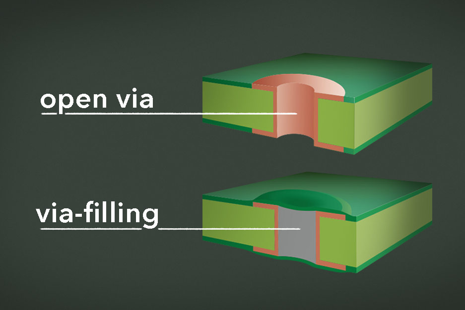
PCB: choose the type of VIA FILLING according to your needs
When we talk about Via Filling in PCBs, we mean a filling process of vias...
Przeczytaj więcej
Checking quality looking “2000 times” more!
We don’t take our eyes off from quality! Our control department is the place where...
Przeczytaj więcej